Samsung Electronics will apply Extreme Ultraviolet (EUV) lithography technology for the first time for DRAM mass production in the memory chip sector to raise efficiency and cut costs, sources close to the matter told The Elec.
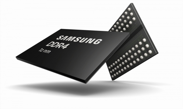
Samsung – the world’s largest memory chipmaker – is scheduled to begin mass producing the 1z-nm, which is its third generation 10nm-class DRAM, starting in September, they said.
Initially, the chipmaker will apply the existing ArF immersion tech to switch to EUV by November, said the sources.
To hedge risks, Samsung will deploy the new technology in intervals. EUV will first be applied will be the BLP layer that touches the bit line. The bit line basically serves as the central data channel. By doing this, the chipmaker can reduce patterning procedures to essentially cut costs.
For ensuing generation of DRAM chips, such as the 1a-nm, Samsung will apply EUV tech to four layers, then five layers for the 1b chip.
Mass production will begin in hand with the foundry business at Samsung’s Hwaseong 17 lines, with EUV applied to the Pyeongtaek lines later on.
Some critics pointed out that the swerve to EUV is not exactly in line with what the world’s largest XX chipmaker said in March when it announced development plans for the 1z. At the time, the company claimed to have enhanced productivity by more than 20 percent compared to the 1y DRAM, and also improved energy efficiency without using EUV equipment.
Samsung’s key crosstown rival SK hynix also plans to apply EUV to as early as its next generation DRAM chips. The firm has been running pilot tests for years.
“Suppliers can also benefit, since DRAM production volume is much higher compared to foundry,” said another market source.
The Elec is Korea's No.1 tech news platform.