[Semicon Korea 2019 Exhibitor]

Nexstin, a specialist in semiconductor inspection and measurement equipment, will try to achieve the Technology Special Listing in the second half of this year.
Park, Tae-hoon, the CEO of Nexstin, said, "Last year, I applied for a designation audit for the KOSDAQ Association for the Technology Special Listing." Park said, "We will focus our efforts on R&D with funds gathered during the listing process."
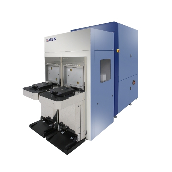
Nexstin is a semiconductor full-process inspection equipment company established in 2010. In 2014, AEGIS, a 2D wafer pattern defect inspection system, was developed for the first time in Korea. Nextin succeeded in supplying to major semiconductor customers.
Identifying micro-defects in wafers is one of the key tasks. As the line width is gradually narrowed, the demand for fine wafer pattern defect inspection increases.
Aegis, the flagship product of Nextin, uses 'deep UV', which is shorter than ultraviolet (UV) and UV, to scan the surface of the wafer and detect defects by comparing it to the finished wafer. The defect is detected by comparing the normal image with the working wafer pattern image. It also contributes to the yield of mass production increase by providing statistical data. It is used in the semiconductor production process of 1x nano or below nodes.
Nextin's patented Dual-Mirror Focal Plane Assembly technology divides the light emitted from a 355-nanometer (nm) high-power pulsed laser into several high-performance image sensors. Thus, wide area inspection is possible at the maximum speed. In Korea, Nextin is the only company with such a technology. Nextin operates a local laboratory in Israel, a powerful image processing technology country, for R&D of inspection equipment.
Nextin will release the Aegis 2, which will further enhance the Aegis inspection capabilities this year. The goal is to complete the development of 3D wafer pattern inspection equipment IRIS, which is a development one step further in 2D. Nextin emphasizes that 3D equipment is capable of a closer inspection of wafer pattern defects by applying multiple unfocused surface imaging techniques.
"We will continue to provide the best defect inspection and measurement solutions," said CEO. "We will grow to be the only company that specializes in measuring and testing equipment in Korea,” he added.


