Samsung Electronics has shared its achievements in localizing its semiconductor component and material supply lines on Thursday.
The South Korean tech giant vowed to continue to work with its subcontractors and academia as well as expand eco-friendly projects.
Samsung said it has co-developed a laser equipment used in DRAM production with vendor EO Technics that the latter previously imported. The equipment has solved a defect issue in DRAM production, the South Korean tech giant said.
Together with subcontractor Cinos, Samsung also developed a ceramic powder used in etching processes in chip production. Similarly, it developed a high selectivity phosphoric acid used in the etching process for NAND flash memory production.
Samsung has also signed an agreement with its equipment vendors such as Wonik IPS, Tes, Eugene Technology, PSK, among others, to co-develop new equipment back in April. The projects will start on July, the company said.
Samsung also donated asher and atomic force microscopy equipments to Korea Polytechnics University. It also opened a new artificial intelligence semiconductor class with Seoul National University.
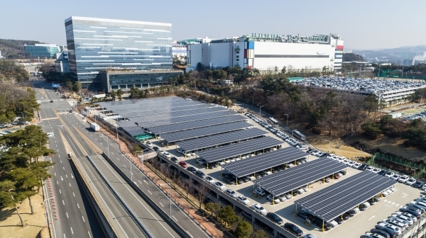
The South Korean tech behemoth said it was working with its surrounding communities to promote protection of the environment. It was building 1500KW solar panel at its campus in Giheung, South Korea. The panels will began supplying power for some parts of the campus in July.
It’s semiconductor businesses’ environment and safety lab was also continuing ways to reduce waste and increase recycling for in its semiconductor production, Samsung added.

