Samsung Electronics is considering investing into its 200mm semiconductor wafer production lines to make it semi-autonomous, TheElec has learned.
The conglomerate’s 300mm wafer lines are currently fully automated. Wafers are transferred from chamber to chamber using over head transport machines.
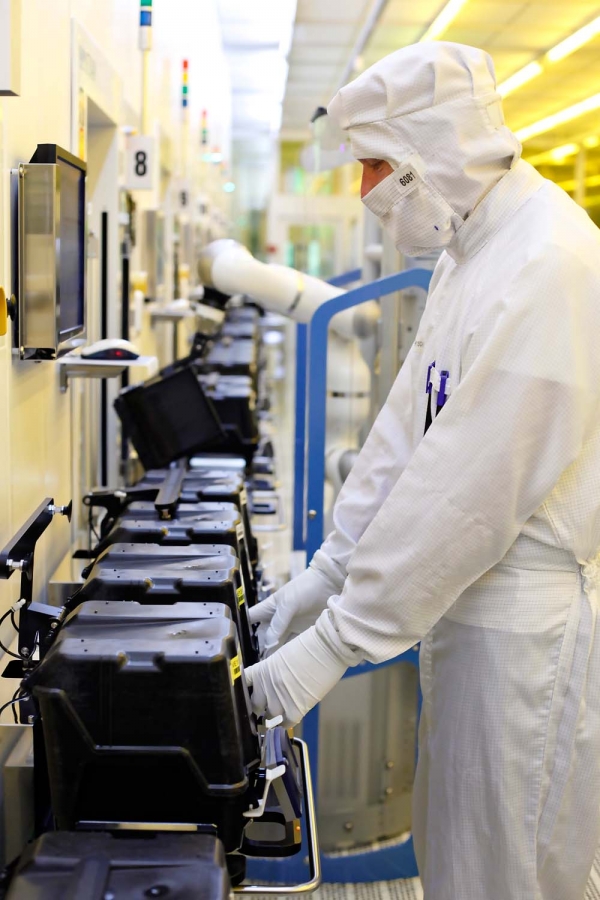
However, for the 200mm lines, wafers inside front opening unified pods (FOUP) are carried by people in carts from chamber to chamber.
Samsung isn’t the only semiconductor company to do this and all companies currently use people to move wafers at 200mm lines.
The South Korean tech giant’s production technology lab currently believes improving this can increase productivity, sources within the company said.
The lab has been researching semi-autonomous equipment. Development of the equipment has been completed recently and they have been deployed to some areas of 200mm lines. The equipment has been well received by the staff at the production line.
The equipment opens the FOUP when they are placed in front of chambers.
Staff will still need to carry wafer FOUP with carts but they will no longer need to open the FOUP and place them on chambers, the sources said. They can just carry the cart and place the FOUP on the designated area near the chamber where the equipment will do the rest.
Samsung is estimating a cost of over 100 billion to deploy machines to every equipment in its 200mm production lines.
There are some who are opposing the idea, raising doubts on whether spending such money on aged equipment in production lines was the right decision.
However, Samsung is also seeing more demand for 200mm foundry from Internet of Things and auto-component sectors __ the wafer size is great for producing small amounts of a variety of different chips.
Samsung’s Giheung fab has lines 5, 6, 7 and 8 that are 200mm lines. It is used to produce eFlash, PMIC, display driver IC, CMOS image sensors, fingerprint readers and microcontroller units. Most of these are for customers. CMOS image sensors is the mainstay for the lines.

