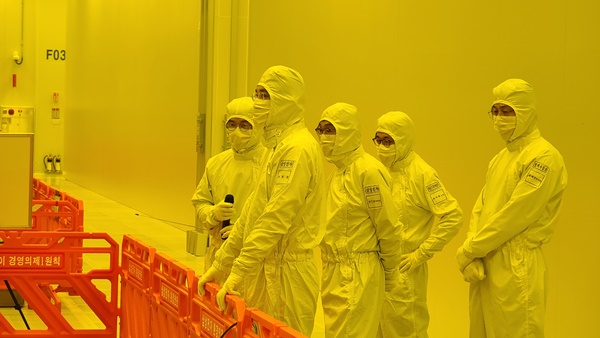
Samsung Electronics said on Monday that vice chairman Lee Jae-yong visited the company’s Pyeongtaek semiconductor plant.
According to Samsung, Lee told executives and employees that they must collaborate with partners, academia and research institutes to build a healthy ecosystem to make history in system semiconductors.
Samsung had invested 30 trillion won in total to the in Pyeongtaek plant’s second factory in 2018. The factory was designed to produce DRAM and V-NAND as well as perform contract chip production using extreme ultraviolet (EUV) process.
Samsung executives and executives of partners participated in an equipment placement ceremony on Monday.
Lee also visited the site of the construction of the third factory at the Pyeongtaek plant and encouraged employees, Samsung said.
Samsung has been co-developing core equipment and components needed in semiconductors with partners since 2010.
The company said in 2019 that it aims to invest 133 trillion won by 2030 to become the world leader in the area by 2030.

