Samsung Electronics’ application of extreme ultraviolet (EUV) lithography technology on its latest DRAM has showed fabrication benefits in scaling, expediting production and improved performance yields, according to reverse engineering analysis firm Techinsights.
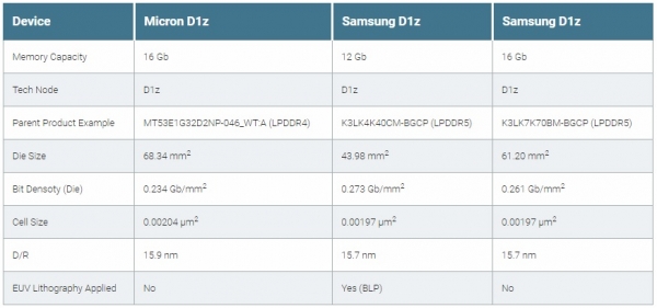
Samsung applied EUV technology on 1znm DRAM, which were found in the company’s latest Galaxy S21 5G smartphone series. The company applied the technology on 1znm 12Gb LPDDR5 chips.
Techinsights’ finding showed that Samsung applied EUV process to one layer __ the BLP (Bit Line Pad). This means the company only used one EUV mask.
Techinsights compared the patterns of a chip with the EUV applied and another that didn’t, which showed that the former has Line Edge Roughness (LER) decreased significantly. This decrease means less short circuit defects.
The firm also compared Samsung’s 1znm 12Gb LPPDR5 with Micron’s 1znm 16Gb LPPDR4.
Samsung’s chip is 12Gb, so comparing the pair’s die size is meaningless, but cell size comparison showed Samsung’s was 3.4% smaller than Micron’s at 0.00197µm².
Samsung’s was also shorter in Design Rule (D/R) by 1.2% at 15.7nm compared to Micron’s 15.9nm. (D/R in DRAM refers to the distance between gates).
Jeongdong Choe, senior tech fellow at Techinsights, wrote on its article on EE Times that reduce DRAM cell size and D/R was becoming increasingly difficult. However, Samsung achieved 15.7nm, which reduce D/R in 1znm DRAM by 8.2% compared to the previous generation 1ynm DRAM.
Companies must approach applying EUV technology to DRAM with an economical perspective, not just reducing circuit width, a person familiar with the matter said. Samsung Electronics and SK Hynix likely considered the economic benefits of applying EUV, despite the initial spending, on specific nodes (1z or 1a) compared to using conventional multi-patterning technology, they said.
Samsung has installed or is installing EUV dedicated production lines at its Hwaseong and Pyeongtaek semiconductor plants. It is already applying EUV to commercial DRAM.
On Wednesday, SK Hynix announced that it was planning to spend 4.75 trillion won up to December 1, 2025 to purchase and install EUV equipment. The company has upgraded its two existing EUV systems, and is planning to apply them at its M16 chip plant, which was completed on February 1 this year. SK Hynix will use EUV to produce Gen 4 1anm DRAM, starting in the second of this year, at the plant.
Choe said Micron will not be applying EUV in its DRAM production for a while, including in 1a and 1b DRAMs.

