A new academic paper shown at SPIE (Society of Photo-Optical Instrumentation Engineers) Advanced Lithography event sheds light on the performance of Nextin’s upcoming 3D wafer pattern inspection equipment Iris.
The paper, called Comparative near infrared through-focus scanning optical microscopy for 3D memory subsurface defect detection and classification, used Nextin’s Iris and Intel’s 3D NAND flash wafer sample and was co-written by Jun Ho Lee, professor at Kongju National University, Naseok Jin and Junhee Jeong of Nextin and Ralf Buengener of Intel. Incheon National University also took part in the research.
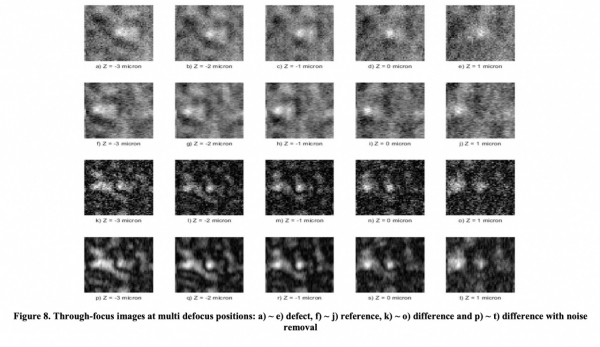
The team used through-focus scanning optical microscopy (TSOM), or scanning of a target through the focus on an optical microscope. They extracted the target TSOM image __ a surface of the die where there could be a defect __ and compare it with an image of an adjacent die that is defect free.
This process allowed the team to detect defects on the subsurface of 3D NAND flash. The method could also be used to guess where the defect is on the die, the team said.
3D NAND flash are comprised of multiple layers of cells. These layers have billions of holes punched through them uniformly from top to bottom. This structure makes it difficult for observers to detect defects within these holes.
Currently, observers can for defects by viewing products from the top and from the bottom. They also cut the 3D NAND flash to sort for defects. This processes takes time and money for vendors. Companies have considered non-optical methods but image processing process such as scanning probe microscopy has proven slow and expensive.
In optical methods, the wavelength of beams must also be shorten to see smaller objects. But when holes are deep, even this can be impractical.
That is why near-infrared (NIR), despite its relatively long wavelength, is used in the industry to look through objects. Nextin’s equipment applied TSOM method to NIR. TSOM is used to film an object multiple times at different focus points to create a 3D video data space. If previous microscopes only used in-focus images, TSOM also applies out-of-focus images to make a 3D data cube. This 3D data cube is used to infer the microscopic shape differences of the structure.
This is the first research in which TSOM method was applied to optical microscopes to detect subsurface defects in 3D NAND flash, professor Lee said. The core technology behind this technology was the software algorithm, he said.
Once the technology is commercialized, it will offer more cost efficient and precise ways to inspect wafer patterns, the professor added.