South Korean chemical firm Miwon Commercial is likely to supply more krypton fluoride (KrF) photoresist polymer to Samsung as the latter upgrades its 3D NAND from Gen 6 to Gen 7, TheElec has learned.
Samsung is preparing to start manufacturing its Gen 7 3D NAND, which has more layers than the previous Gen 6 128-layer 3D NAND that is currently commercialized.
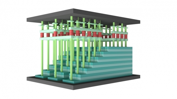
For Gen 7, the South Korean tech giant is also preparing to connect two 3D NAND dies __ a technique called double stacking. This means more production materials will be needed per layer than previously.
Miwon started supply the polymer used in thick KrF photoresist to Dongjin Semichem in 2019. Dongjin then supplies the material to Samsung for use in NAND production.
Dongjin previously procured KrF photoresist polymer from NC Chem up to the use for 96-layer NAND, but it changed its supplier to Miwon starting with 128-layer. Around 25 billion won to 30 billion won worth of this material for photoresist is used per year, people familiar with the matter said.
It is not well known that Miwon supplies the polymer in KrF photoresist Samsung uses for its Gen 6 128-layer 3D NAND flash, the people said.
For Gen 7, there maybe some competitors to Miwon that will also supply the material to the South Korean tech giant, they said. However, as the overall volume will go up, Miwon will likely see significant sales growth from the product going forward nonetheless, they added.
Photoresist are used in the lithography process in semiconductor production. The patterns on the wafer are made through the laser’s reaction with the photoresist.
Photoresist is composed of polymer, photo acid generator and solvent.
For 3D NAND flash production, thick photoresists are used over conventional photoresists to increase speed of the process. The multiple layers on the chip are made simultaneously, and they are cut simultaneously as well.
Being thick means the material has high viscosity. The higher the viscosity, the lower the uniformity gets, meaning the technology needed to make the material is quite sophisticated.
Samsung has been collaborating with Dongjin to develop thick KrF photoresist before the company began production of its Gen 1 3D NAND in 2013.
Samsung procures the material exclusively from Dongjin. Dongjin also only supplies them to Samsung.
Miwon previously focused on supplying chemicals for the back-end processes of semiconductor production but is finding success in front-end processes like photoresist, another person familiar with the matter said. The firm will likely see more sales from supplying materials used in semiconductor production going forward.


