Samsung Electronics plans to diversify its supply of photoresists (PR), one of the core materials used in the 3D NAND flash production process. It means the exclusive supply system will be no longer valid for use by Dongjin Semichem, which has been in operation for more than five years.
According to the industry, on the 18th, Samsung Electronics is reported to be evaluating the application of krypton fluoride (KrF) PR materials from the Tokyo Ohka Kogyo (TOK) of Japan to the mass production line. TOK is the No. 1 company of the worldwide semiconductor PR material market. It has focused on its capability to supply PR materials for 3D NAND flash production of Samsung Electronics so far.
An industry insider explained, "I’m aware that TOK mostly met the requirements of Samsung Electronics," and "it is reliable enough to be used in the next generation of product production."
PR is the key material used in the exposure process. Exposure refers to a series of processes to form a circuit pattern by illuminating the mask plate which is engraved on the design pattern with metals. The light transmitted through the mask reacts with the PR to form a pattern.
The exposure process is divided into generations according to the type of light source. A krypton fluoride(KrF) excimer laser with a wavelength of 248 nanometers(nm) was used on up to a 130 nanometer semiconductor. As the range of 90-nanometers emerged, Argon fluoride(ArF) excimer laser with a wavelength of 193nm started being used. Since then, the immersion ArF equipment has been commercialized to enhance resolution by using a liquid medium with a higher refractive index than air. Currently, the exposure equipment used in most of the latest semiconductor production lines is the immersion ArF. Exposure equipment of the extreme ultraviolet lithography(EUV) which will be utilized as a short wavelength of 13.5nm in the production of the system semiconductors of 7nm and less, is expected to start being operated in the mass production line soon.
If the light sources of the exposure equipment are changed, the material should also be adjusted to be used in accordance with to the change. For 3D NAND flash, it is important to stack a high-level, but narrowing the line width like as in the case of 2D won’t be a main consideration. Therefore, KrF is more widely used for exposure than ArF. However, the caliper of the KrF material used in this case should be thicker unlikely existing cases when applied.
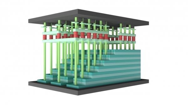
"If you want to build a 100-layer 3D NAND, you have to form 100 stairs. If you build one at a time, the cost will go up too much," said Kang Ho-kyu, director of the semiconductor research at Samsung Electronics (vice president). He also explained “By utilizing an extremely thick PR, it’s possible to form multiple stairs.”
Samsung Electronics collaborated with Dongjin Semichem to develop a thick KrF before mass production of first-generation 3D NAND flash in 2013. To apply something as a thick layer means it must have a high viscosity. It is not easy to develop a highly viscous material because the uniformity is lowered when it is applied. Samsung Electronics cooperated with Dongjin Semichem thoroughly and encouraged development by opening all "confidential" process recipes. As a result, Dongjin Semichem succeeded in developing materials with a thickness of 30% and more compared to that of existing KrF PR.
Currently, Dongjin Semichem supplies this material only to Samsung Electronics. And in turn, Samsung Electronics uses only Dongjin Semichem materials. This will be the identical context for which Samsung Electronics invested 25.1 billion KRW in Dongjin Semichem in October last year. Dongjin Semichem's supply price to Samsung Electronics was too low, so there was no opportunity for competitors to come between this business relationship.
An industry insider said, "As the number of 3D NAND flash stacks increases, there is a growing number of manufacturers adopting the Double Stacking method", and “Samsung is planning to procure the TOK ‘s materials in order to stick to the Single Stacking.”
Double Stacking is a technique of stacking two stacked 3D NAND flashes, which completed the stacking task, to increase the number of layers. There is an insulating shield between two. SK Hynix's 72-layer NAND flash is made by attaching two 36-layer products. Double Stacking includes a larger number of processes and more materials than the Single Stacking method which stacks cells solely.


