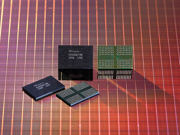
SK Hynix has begun the production of 10-nanometer (1a) 8Gb LPDDR4 mobile DRAM this month, the company said on Monday.
It was also applying the extreme ultraviolet (EUV) process for the memory, SK Hynix aid.
It is the first time that SK Hynix has applied EUV in its DRAM production. The new chip will be supplied to smartphone manufacturers starting in the second half of the year.
SK Hynix will also be applying 1a-nm and EUV for DDR5 chips that it will start manufacturing in early 2022.
There are two things to note here, according to experts TheElec has talked to:
Firstly, that EUV process has been applied successfully. EUV its an exposure technology used in the lithography process. EUV offers higher resolution compared to the previously widely used exposure technology, which is argon fluoride immersion. Previously, chip companies had to conduct double patterning or even quadruple patterning to make up for the relatively lower resolution transferred on to the wafer. EUV can do this in a single step. However, EUV equipment and required infrastructure is expensive. Additionally, chip companies can face yield issues in their first adoption of the technology.
EUV equipment, which is solely supplied by the Netherlands’ ASML, costs around 150 billion won to 200 billion won per unit, and requires a lot of experience to operate, one of the experts said.
For this reason, DRAM companies are planning to apply EUV for a few important one to four layers, then gradually expand its application, they said.
Earlier this year, SK Hynix had said it plans to spend 4.75 trillion won by the end of 2025 to secure EUV equipment.
The company had used its newly applied EUV equipment for the 8Gb LPPDR4 mobile DRAM, another person familiar with the matter said. SK Hynix is also planning to upgrade its two existing EUV equipment that it had used for research purposes to apply them commercially at a later date.
Secondly, SK Hynix has secured productivity. The company has used its fourth-generation 10-nm process (1a, previous generations were called 1z, 1y and 1x, which were the third, second and first generations, respectively) for the latest chip. It said it has produced 25% more units of DRAM from a single wafer compared to the prior generation of 10-nm. This will give SK Hynix and advantage in cost.
Cho Youngmann, vice president at SK Hynix, said: “With improved productivity and cost competitiveness, the latest 1anm DRAM will not only help secure high profitability, but also solidify SK Hynix’s status as a leading technology company with early adoption of the EUV lithography technology for mass production.”
Samsung applied EUV for the first time with its third-generation 10-nm DRAM. It is planning expand their application for the next-generation 10-nm. Micron recently said it plans to apply EUV in DRAM production in 2024.

