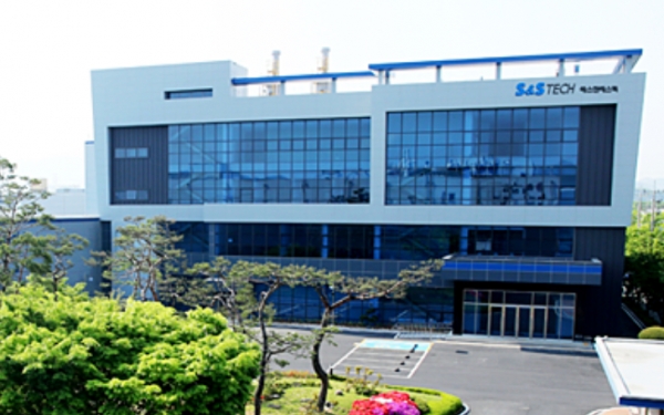
South Korean blank mask maker S&S Tech has succeeded in developing a pellicle used in the extreme ultraviolet (EUV) process during wafer fabrication with 90% light transmittance, TheElec has learned.
The company is the first in South Korea to develop a full-sized EUV pellicle.
ASML, the sole manufacturer of EUV equipment, has also developed its own EUV pellicle with over 90% transmittance to sell to customers.
S&S Tech was in talks with ASML to hold quality testing for the EUV pellicle it developed, people familiar with the matter said.
Pellicle is used to protect the photo mask from dust during the lithography process in wafer fabrication, where the chip design is imprinted on the silicon wafer.
More memory chip makers are expanding the application of EUV equipment to their production, increasing demand for the pellicles.
EUV equipment reflects the light it shoots before it reaches the wafer, unlike ArF equipment that shoots the light directly.
These reflections mean the light can get weakened, so pellicles used in EUV process but have a high light transmittance rate of over 90%.
Companies can choose not to use pellicles but EUV masks are incredibly expensive so it is better to use them to protect them so that they can be used longer.
S&S Tech’s EUV pellicle showed a transmittance of between 89% to 90%, the people said.
However, it is guaranteeing up to 85% transmittance. The pellicle is expected to endure for between 10,000 to 20,000 hours of use.
Meanwhile, compatriot FST is also developing EUV pellicles. ASML has recently succeeded in developing one with 90.6% transmittance, which will be supplied to Samsung Electronics.
The South Korean tech giant is planning to apply pellicles in a larger scale in its EUV processes starting at the end of 2023.
SK Hynix and Micron are also planning to expand their use of EUV processes for their respective chip production, while will increase demand for pellicles.

