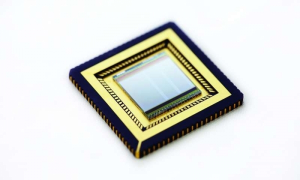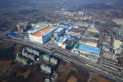
SK Hynix produces a 2-layer stacked CMOS Image Sensor (CIS) at its 300mm wafer plant. This is SK Hynix’s first time to produce a stacked CIS.
According to a industry report on the 25th, SK Hynix plans to mass-produce a 16 megapixel, 2-layer stacked CIS using the Through Silicon Via (TSV) technology in the M10 line in Icheon, Gyeonggi-do in the first half of next year. It is expected to be installed in Huawei, Samsung Electronics, and LG Electronics’ low- and middle-priced smartphones. The 2-layer stacked CIS is the first in SK Hynix's history. The new product also incorporates Phase Detection Auto Focus (PDAF) technology. PDAF is a type of technology that compares the phase difference and rapidly brings a camera into focus by dividing the light coming into the lenses to one pair
The 2-layer stacked CIS was first introduced in 2013 by Sony. In 2017, the technology advanced to the point of the successful development of a 3-layer stacked CIS capable of superhigh-speed shooting with the addition of DRAM. Samsung Electronics has applied the 3-layer stacked CIS to the Galaxy S9, which launched this year.
Over the past few years, SK Hynix has focused on improving pixel density while improving the dark current, one of the challenges of BackSide Illumination (BSI)-CIS. Dark current is a phenomenon in which there is a flow of current even when no light reaches the lens. Naturally, noise and horizontal lines (cross talk) occur which decrease the image quality. These are the side effects caused by increasing transistor density of the same size (plate type) to make higher resolution. It may be solved by altering the plate type, however it becomes difficult to install in narrow smartphones. This is why stacking through TSV is necessary. The 2-layer stacked CIS includes the identical plate type as the existing 1300 megapixel CIS. The pixel size is 1㎛.

Mass production is intended for next year, but the timing may be changed according to clients’ schedule. First of all, the M10 will begin mass production within the year starting from 1300-megapixel products. When mass production of the CIS takes place at the M10, production of low-cost products under 800-megapixels will be incorporated into the M8, a 200 mm wafer fab in Cheongju. As the wafer grows from 200mm to 300mm, the amount of chip production will increase by 50%. Because the earnings rate rises, the proportional amount of M8's total CIS production will gradually decrease.
One industry insider mentioned "A 3-layer stacked CIS even with DRAM will be the next target," and "since PDAF has been properly applied from the beginning of this year, the 3-layer stacked CIS is likely to be applied after improving the 1600-megapixel version multiple times."

