Experts say high-NA EUV components needed

Extreme ultraviolet (EUV) equipment will account for over 60% of the lithography equipment used in wafer fabrication by 2025, according to an executive of fab equipment firm ASML.
Speaking at the 2021 Semiconductor EUV Ecosystem Big Trend Relay Conference hosted by TheElec and the Korea Semiconductor Industry Association on Wednesday, ASML senior market manager Lee Sung-woo said the company is forecasting that the worldwide semiconductor market will grow 7.4% from 2020 to 2025.
Logic chip, DRAM and NAND markets will grow 10.9%, 5.7% and 6.3%, respectively, over that same time period, Lee said.
EUV equipment use in these sectors will grow steadily over the next five years, eventually accounting for 60% of the lithography equipment used in the overall semiconductor market, the manager said.
Chip giants such as Samsung Electronics, TSMC and Intel have begun applying EUV equipment to their wafer fabrication.
The kit is used in the production of the latest and most advanced chips as the kit allows these companies to draw finer blueprints of the chips they want to manufacture on wafers.
Dutch firm ASML is currently the sole manufacturer of EUV equipment.
Also speaking at the conference, Hanyang University division of materials science and engineering professor Jinho Ahn said there need to be a lot more improvements in the performance of materials and components used in EUV process.
EUV kits, which started being used in the non-memory sector, are seeing a rapid demand increase in the memory sectors recently, the professor said.
But South Korean chip companies were wholly reliant on imports for all this EUV, from materials, components and equipment, and the country needs to foster more related companies, Ahn noted.
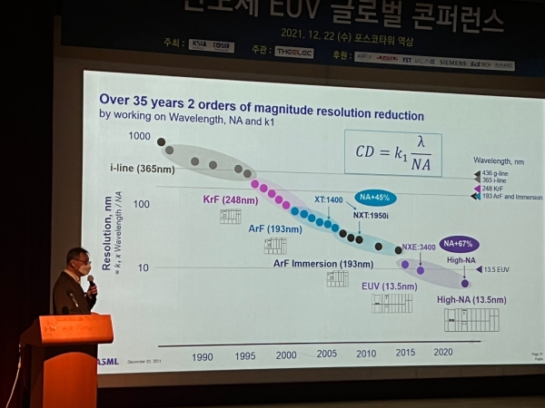
The professor also stressed that South Korean chip companies needed to prepare for ASML’s next EUV equipment, which is the high-NA EUV kit.
ASML’s current EUV kits are 0.33 NA, but it is planning to start developing of equipment with 0.55 NA in 2023.
Intel had previously said it is planning to apply the equipment to its wafer fabrication in 2023.
NA, or numerical aperture, refers to the size of the lens on the equipment. A large lens means it can collect more light, which will allow for clearer and more precise lithography.
Ahn noted that high-NA EUV will require the development of accompanying masks and pellicles, which will give opportunities for South Korean companies to develop them to take part in the EUV market’s growth.

