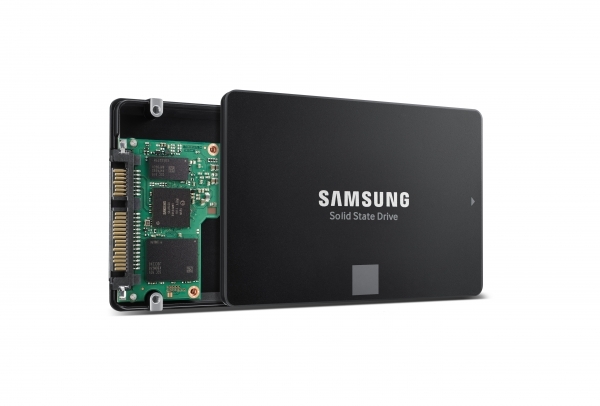
Samsung Electronics, the world’s largest memory chipmaker, said on Aug. 6 it has succeeded in mass producing 250Gb SATA solid state drives (SSD) integrating the company’s 6th-generation (1xx-layer) 256Gb three-bit V-NAND to be supplied to global PC makers.
By launching a new generation of V-NAND in just 13 months, Samsung has slashed the mass production cycle by four months, the company said. It has also managed to achieve the industry’s highest performance, power efficiency and manufacturing productivity.
“By bringing cutting-edge 3D memory technology to volume production, we are able to introduce timely memory lineups that significantly raise the bar for speed and power efficiency,” said Kye Hyun-kyung, executive vice president of Solution Product & Development at Samsung Electronics in a press release.
“With faster development cycles for next-generation V-NAND products, we plan to rapidly expand the markets for our high-speed, high-capacity 512Gb V-NAND-based solutions.”
Samsung’s 6th-generation V-NAND currently features the industry’s fastest data transmission rates.
By utilizing “channel-hole etching” technology, the new V-NAND adds around 40% more cells to the previous 9x-layer single-stack structure. This was achieved by building an electrically conductive mold stack comprised of 136 layers, then vertically piercing cylindrical holes through them to to form 3D charge trap flash (CTF) cells.
To overcome shortcomings such as more errors and read latencies in NAND flash chips that occur when the mold stack in each cell rises in height, Samsung incorporated a speed-optimized circuit design to achieve the fastest data transfer speed of below 450 microseconds (μs) for write operations and below 45μs for reads. Compared to the previous generation, this reflects a minimum 10% improvement in performance, while power consumption is down by more than 15%.
Thanks to this speed-optimized design, Samsung said it can offer next-generation V-NAND solutions with over 300 layers just by mounting three of the current stacks without compromising chip performance or reliability.
In addition, the number of channel holes required to create a 256Gb chip density was cut to 670 million holes from over 930 million that has improved manufacturing productivity by more than 20%.
The tech giant now plans to expand its 3D V-NAND into areas like next-generation mobile devices, enterprise servers, and also the automotive market.
In the latter half of the year, Samsung plans to offer 512Gb three-bit V-NAND SSD and eUFS, while also producing more of the 6th-generation V-NAND solutions at its Pyeongtaek campus starting next year.
The Elec is South Korea’s No.1 tech news platform.

