[Semicon Korea 2019 Exhibitor]

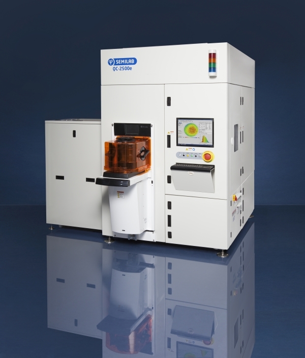
SemiLAB Korea is speeding up to take the semiconductor market with infrared (IR) measurement equipment. This is thanks to the unique commercialization of its IR measurement equipment using long wavelengths. SemiLAB has proposed a method for precisely measuring DRAM and NAND flash structures that has become increasingly complex. The company also has raised its sales target to 20 billion won for this year (14 billion won last year) and 26 billion won for the next year.
SemiLAB Korea is headquartered in Budapest, the capital of Hungary. It was established in 1988 and established a corporate branch in Korea in 2009. It has achieved sales of 150 billion won over the past 10 years and is the second largest after China. Initially, SemiLAB started with a deep level transient spectroscope (DLTS) instrument to identify deep traps, which are defects that are unintentionally created by impurities or heat treatments contained in semiconductors. In 2009, through hostile takeovers, it was able to take both of the solar and semiconductor markets.
The representative products of this year are measuring instruments using IR technology. It is possible to monitor BPSG (boro-phospho silicate glass) and NAND flash etch (Etch) processes used as insulation films before DRAM capacitors are made. SemiLAB Korea CEO, Park, Soo-yong, emphasized, "IR, because it has longer wavelengths, can look at thin film structures that become more complex,” and added, "Many materials are piled up or the composition of the film changes, so the usage tendency is becoming diversified."
For example, DRAMs actively apply high dielectric constant (H-K) materials among the dielectric materials to improve capacitor performance. High-K is literally a material with a high dielectric constant. The higher the value of 'K', the more leakage current (tunneling phenomenon) is prevented and the better gate insulation characteristic is, thus, microcircuits can be made easily. Until now, it has been developed while improving the characteristics of zirconium (Zr) based high-K, but it mixes different materials or uses completely new materials. It means that the material layer has become thicker.
The IR measurement equipment is based on the model and measures reflectivity to improve accuracy and reliability. Epitaxy thickness can be optically examined. Thus, it is possible to obtain an absolute value that can grasp the semiconductor characteristics. CEO Park said, "Because there are parts that the conventional measuring equipment cannot look into, which influences the yield, and the interest is growing."
It also has monitoring equipment using non-optical electrical characteristics. Semiconductors repeat the process of taking (exposure), shaving (etching), washing (cleaning), covering (depositing), and implanting impurities. If impurities are left unintentionally in this process, it affects the next process. Even the impurities are left at the atomic level, the inside of the chamber has extremely high temperature and high pressure that it can increase the wafer defect rate.
CEO Park said, “Because high-temperature work is prevalent these days, reports have been made of oxygen spreading more than expected,” and he explained, "NAND flash and system semiconductors are relatively inexperienced than DRAM, resulting in poor yields due to cleaning and residual contaminants.”
Meanwhile, SemiLAB Korea plans to increase the supply of standardized equipment to not only the semiconductor but also the solar cell and display markets. It is a strategy to build reliability by constantly supplying measurement equipment utilizing optical and electrical characteristics.


