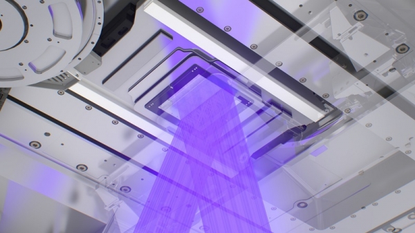
Samsung and SK Hynix are expanding their use of extreme ultraviolet (EUV) lithography as they transition to the production of more and more advanced DRAM.
This means demand for high-purity carbon dioxide (CO2) gases is also expected to increase. These gases are used to make the light source used in EUV processes.
Samsung and SK Hynix have begun the production of their respective Gen 5 10-nanometer (nm) DRAMs.
These nodes, either 1a or 1b, have four to five EUV layers, more than the previous 1z node which only had one EUV layer.
Samsung said back in January during the conference call for the fourth quarter that 1a DDR5 DRAM accounted for over half of its server DRAM shipment.
SK Hynix also said that it was aiming to shift its DRAM to the 1a node so that it can produce DDR5 and LPDDR5 chips.
These statements mean the chipmakers are planning to increase the use of EUV processes.
EUV light are made by amplifying the laser from the EUV light source at a vacuum state and irradiating the emitted light on tin. The tin turns to gas at this moment a short wavelength EUV light is formed. Adding CO2 during this process causes a plasma to occur.
SK Hynix is planning to install at least 5 units of additional EUV machinery this year. Samsung already uses over 40 units of EUV equipment.

