LG Innotek is considering developing glass substrates for use in chip packaging, a company official said.
LG Innotek general manager Jaeman Park said on Wednesday during the SMT&PCB Tech Conference hosted by TheElec in Suwon that glass is likely to become the main ingredient in the future for substrates used in semiconductor packaging. Because of this trend, the South Korean electronics parts maker was also reviewing the development of glass substrates, he said.
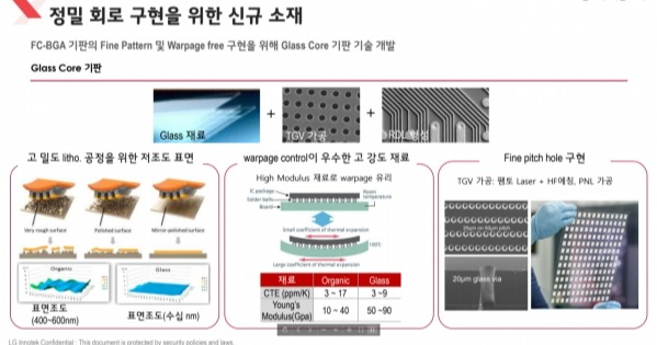
Currently, most substrates used in chip packages are made out of plastic. Glass has superior characteristics compared to plastic in terms of response to temperature changes and signals so it is easier to make smaller and wider, Park said.
Glass substrates are in demand for use in packages for server CPU and AI accelerators as well as other high-end chips. Park told the conference that lead frames, or metals, were used as substrates in the past but this changed to ceramic then later plastic in the 2000s.
Glass was proposed as the next big thing by the Georgia Institute of Technology in 2010 but at the time it was unrealistic; but now most companies believe glass will become the next-generation material to be used in substrates, the general manager said.
Intel has been the most active in pursuing the commercialization of glass substrates today. Absolics, a subsidiary of SKC, is developing glass substrates based on the technology proposed by the Packaging Research Center of Georgia Tech. The company is planning to start construction of a factory for glass substrates in Covington, Georgia.
Samsung Electro-Mechanics is also planning to build a glass substrate production line this year to manufacture a prototype in 2025 and start mass production in 2026, company CEO Chang Duckhyun said during CES earlier this year. Japan’s Dai Nippon Printing also said last year in March that it developed its own glass core substrate and said it believes glass will replace resin in high-end chip packages such as flip chip ball grid arrays.
According to Park, in a glass substrate, the glass is in the center and Ajinomoto Build-Up Film or another kind of insulator film is laid on top of it. Because the glass is in the center, it is free from warpage. A glass substrate’s Young’s Modulus is around 70 to 80; four times the 20 of other substrates made with organic material, the general manager noted. Glass also has a low coefficient of thermal expansion, making it an optimal match with a silicon chip, he said, while they are also convenient to punch in narrow holes, he added.